- 您现在的位置:买卖IC网 > Sheet目录342 > MCBSTM32EXL (Keil)BOARD EVALUATION FOR STM32F103ZE
�� �
�
�RM0008�
�Flexible� static� memory� controller� (FSMC)�
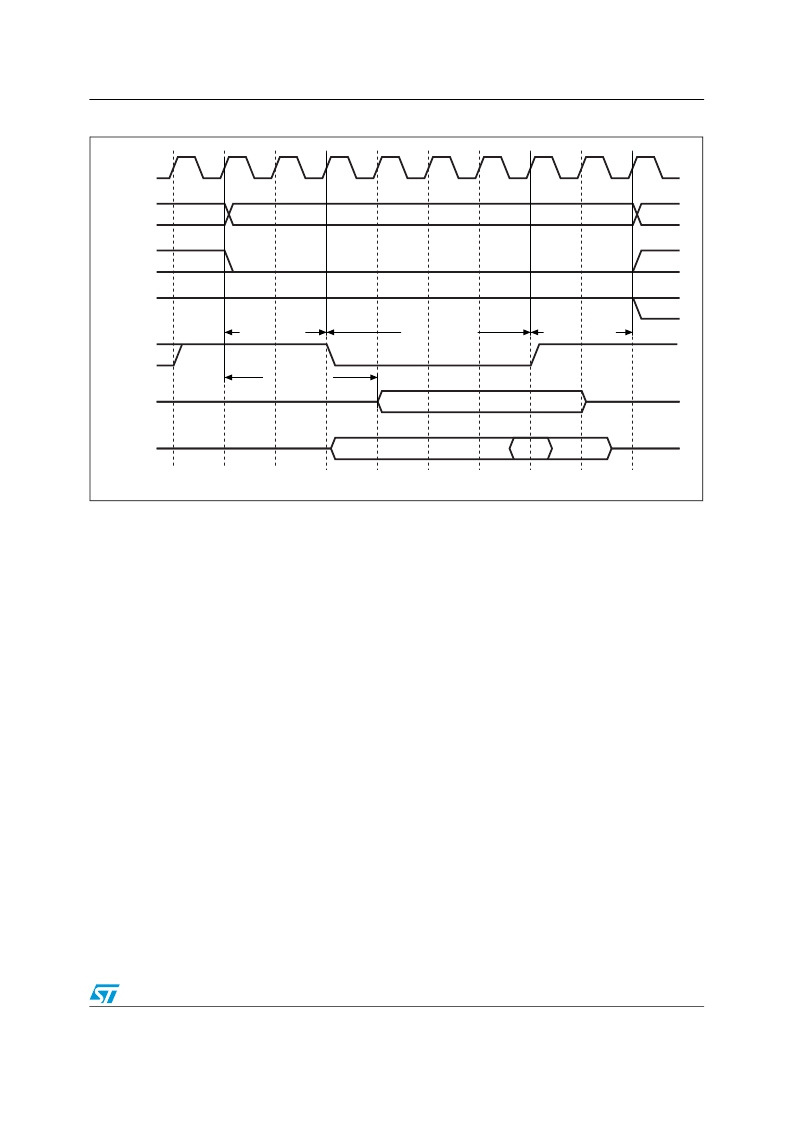
�Figure� 175.� NAND/PC� Card� controller� timing� for� common� memory� access�
�HCLK�
�A[25:0]�
�NCEx� (2)�
�NREG,� High�
�NIOW,�
�NIOR�
�NWE,�
�NOE� (1)�
�write_d� a� t� a�
�re� a� d_d� a� t� a�
�MEMx� S� ET� +� 1�
�MEMxHIZ� +� 1�
�MEMxWAIT� +� 1�
�V� a� lid�
�MEMxHOLD� +� 1�
�a� i147� 3� 2c�
�1.� NOE� remains� high� (inactive)� during� write� access.� NWE� remains� high� (inactive)� during� read� access.�
�2.� NCEx� goes� low� as� soon� as� NAND� access� is� requested� and� remains� low� until� a� different� memory� bank� is� accessed.�
�19.6.4�
�NAND� Flash� operations�
�The� command� latch� enable� (CLE)� and� address� latch� enable� (ALE)� signals� of� the� NAND�
�Flash� device� are� driven� by� some� address� signals� of� the� FSMC� controller.� This� means� that� to�
�send� a� command� or� an� address� to� the� NAND� Flash� memory,� the� CPU� has� to� perform� a� write�
�to� a� certain� address� in� its� memory� space.�
�A� typical� page� read� operation� from� the� NAND� Flash� device� is� as� follows:�
�1.�
�2.�
�3.�
�Program� and� enable� the� corresponding� memory� bank� by� configuring� the� FSMC_PCRx�
��Flash� pre-wait� functionality� on� page� 446� )� registers� according� to� the� characteristics� of�
�the� NAND� Flash� (PWID� bits� for� the� databus� width� of� the� NAND� Flash,� PTYP� =� 1,�
���The� CPU� performs� a� byte� write� in� the� common� memory� space,� with� data� byte� equal� to�
�one� Flash� command� byte� (for� example� 0x00� for� Samsung� NAND� Flash� devices).� The�
�CLE� input� of� the� NAND� Flash� is� active� during� the� write� strobe� (low� pulse� on� NWE),� thus�
�the� written� byte� is� interpreted� as� a� command� by� the� NAND� Flash.� Once� the� command�
�is� latched� by� the� NAND� Flash� device,� it� does� not� need� to� be� written� for� the� following�
�page� read� operations.�
�The� CPU� can� send� the� start� address� (STARTAD)� for� a� read� operation� by� writing� four�
�bytes� (or� three� for� smaller� capacity� devices),� STARTAD[7:0],� then� STARTAD[16:9],�
�STARTAD[24:17]� and� finally� STARTAD[25]� for� 64� Mb� x� 8� bit� NAND� Flash)� in� the�
�common� memory� or� attribute� space.� The� ALE� input� of� the� NAND� Flash� device� is� active�
�during� the� write� strobe� (low� pulse� on� NWE),� thus� the� written� bytes� are� interpreted� as�
�Doc� ID� 13902� Rev� 9�
�445/995�
�发布紧急采购,3分钟左右您将得到回复。
相关PDF资料
MCBTMPM330
BOARD EVAL TOSHIBA TMPM330 SER
MCIMX25WPDKJ
KIT DEVELOPMENT WINCE IMX25
MCIMX53-START-R
KIT DEVELOPMENT I.MX53
MCM69C432TQ20
IC CAM 1MB 50MHZ 100LQFP
MCP1401T-E/OT
IC MOSFET DRVR INV 500MA SOT23-5
MCP1403T-E/MF
IC MOSFET DRIVER 4.5A DUAL 8DFN
MCP1406-E/SN
IC MOSFET DVR 6A 8SOIC
MCP14628T-E/MF
IC MOSFET DVR 2A SYNC BUCK 8-DFN
相关代理商/技术参数
MCBSTM32EXLU
功能描述:开发板和工具包 - ARM EVAL BOARD + ULINK2 FOR STM32F103ZG
RoHS:否 制造商:Arduino 产品:Development Boards 工具用于评估:ATSAM3X8EA-AU 核心:ARM Cortex M3 接口类型:DAC, ICSP, JTAG, UART, USB 工作电源电压:3.3 V
MCBSTM32EXLU-ED
制造商:ARM Ltd 功能描述:KEIL STM STM32EXL EVAL BOARD
MCBSTM32EXLUME
功能描述:开发板和工具包 - ARM EVAL BOARD + ULINKME FOR STM32F103ZG
RoHS:否 制造商:Arduino 产品:Development Boards 工具用于评估:ATSAM3X8EA-AU 核心:ARM Cortex M3 接口类型:DAC, ICSP, JTAG, UART, USB 工作电源电压:3.3 V
MCBSTM32F200
功能描述:开发板和工具包 - ARM EVAL BOARD FOR STM STM32F207IG
RoHS:否 制造商:Arduino 产品:Development Boards 工具用于评估:ATSAM3X8EA-AU 核心:ARM Cortex M3 接口类型:DAC, ICSP, JTAG, UART, USB 工作电源电压:3.3 V
MCBSTM32F200U
功能描述:开发板和工具包 - ARM EVAL BOARD FOR STM STM32F207IG + ULINK2
RoHS:否 制造商:Arduino 产品:Development Boards 工具用于评估:ATSAM3X8EA-AU 核心:ARM Cortex M3 接口类型:DAC, ICSP, JTAG, UART, USB 工作电源电压:3.3 V
MCBSTM32F200UME
功能描述:开发板和工具包 - ARM EVAL BOARD FOR STM STM32F207IG ULINK-ME
RoHS:否 制造商:Arduino 产品:Development Boards 工具用于评估:ATSAM3X8EA-AU 核心:ARM Cortex M3 接口类型:DAC, ICSP, JTAG, UART, USB 工作电源电压:3.3 V
MCBSTM32F200UME-ED
制造商:ARM Ltd 功能描述:KEIL STM32F207IG EVAL BOARD
MCBSTM32F400
功能描述:开发板和工具包 - ARM EVAL BOARD FOR STM STM32F407IG
RoHS:否 制造商:Arduino 产品:Development Boards 工具用于评估:ATSAM3X8EA-AU 核心:ARM Cortex M3 接口类型:DAC, ICSP, JTAG, UART, USB 工作电源电压:3.3 V